| Sign In | Join Free | My howtoaddlikebutton.com |
|
| Sign In | Join Free | My howtoaddlikebutton.com |
|
| Categories | Silicon Carbide Wafer |
|---|---|
| Brand Name: | ZMSH |
| Place of Origin: | China |
| MOQ: | 1 |
| Price: | by case |
| Payment Terms: | T/T |
| Supply Ability: | By case |
| Delivery Time: | 2-4 weeks |
| Packaging Details: | custom cartons |
| Polytype: | 4H |
| Doping Type: | N-type |
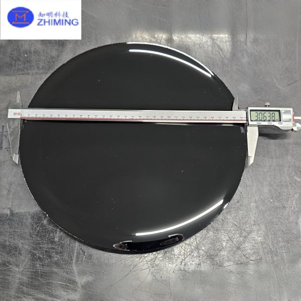
| Diameter: | 300 ± 0.5 mm |
| Thickness: | Green: 600 ± 100 µm / White-transparent: 700 ± 100 µm |
| Surface Orientation (Off-cut): | 4° toward \<11-20\> ± 0.5° |
| TTV (Total Thickness Variation): | ≤ 10 µm |
| Company Info. |
| SHANGHAI FAMOUS TRADE CO.,LTD |
| Verified Supplier |
| View Contact Details |
| Product List |
The 12-inch Silicon Carbide (SiC) wafer represents the next generation of wide bandgap semiconductor substrates, designed to support the large-scale production of high-performance power electronic devices. Compared with conventional 6-inch and 8-inch SiC wafers, the 12-inch format significantly increases usable chip area per wafer, improves manufacturing efficiency, and offers strong potential for long-term cost reduction.
Silicon carbide is a wide bandgap semiconductor material featuring high breakdown electric field strength, excellent thermal conductivity, high saturated electron drift velocity, and outstanding thermal stability. These properties make 12-inch SiC wafers an ideal platform for high-voltage, high-power, and high-temperature applications.

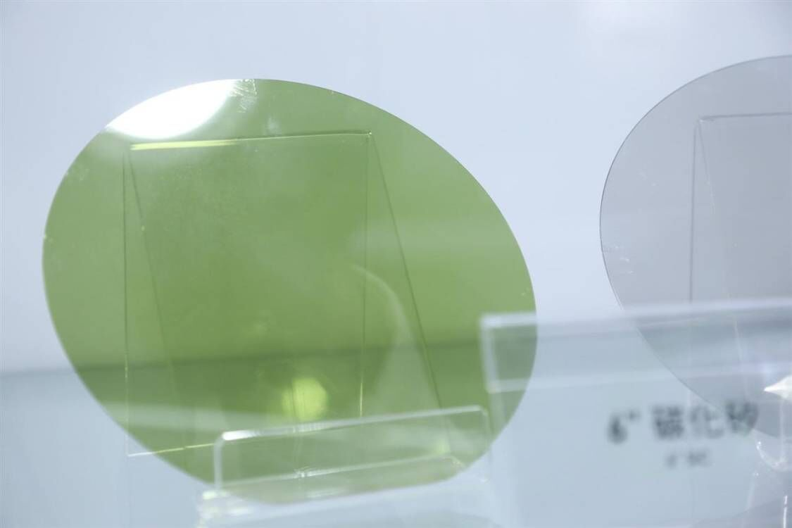
Material: Single-crystal Silicon Carbide (SiC)
Polytype: 4H-SiC (standard for power devices)
Conductivity Type:
N-type (Nitrogen doped)
Semi-insulating (customizable)
The growth of 12-inch SiC single crystals requires advanced control of temperature gradients, stress distribution, and impurity incorporation. Improved PVT (Physical Vapor Transport) crystal growth technology is typically employed to achieve large-diameter, low-defect SiC boules.

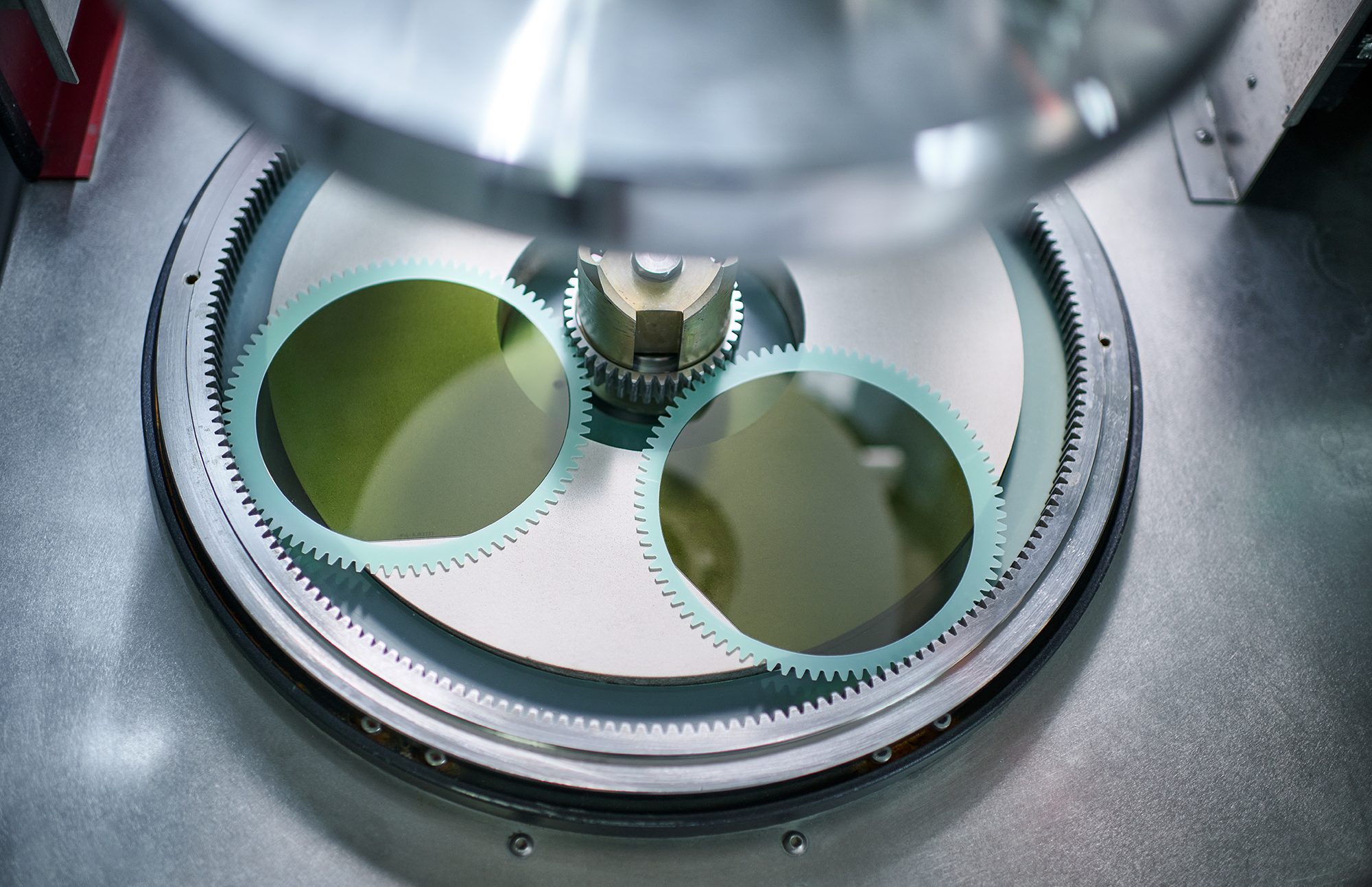
The production of 12-inch SiC wafers involves a series of high-precision processes:
Large-diameter single-crystal growth
Crystal orientation and ingot slicing
Precision grinding and wafer thinning
Single-side or double-side polishing
Advanced cleaning and comprehensive inspection
Each step is tightly controlled to ensure excellent flatness, thickness uniformity, and surface quality.
Higher Device Yield per Wafer: Larger wafer size enables more chips per run
Improved Manufacturing Efficiency: Optimized for next-generation fabs
Cost Reduction Potential: Lower cost per device in high-volume production
Superior Thermal and Electrical Performance: Ideal for harsh operating conditions
Strong Process Compatibility: Suitable for mainstream SiC power device fabrication
Electric vehicles (SiC MOSFETs, SiC Schottky diodes)
On-board chargers (OBC) and traction inverters
Fast-charging infrastructure and power modules
Solar inverters and energy storage systems
Industrial motor drives and railway systems
High-end power electronics and defense applications
| Item | N-type Production Grade (P) | N-type Dummy Grade (D) | SI-type Production Grade (P) |
|---|---|---|---|
| Polytype | 4H | 4H | 4H |
| Doping Type | N-type | N-type | / |
| Diameter | 300 ± 0.5 mm | 300 ± 0.5 mm | 300 ± 0.5 mm |
| Thickness | Green: 600 ± 100 µm / White-transparent: 700 ± 100 µm | Green: 600 ± 100 µm / White-transparent: 700 ± 100 µm | Green: 600 ± 100 µm / White-transparent: 700 ± 100 µm |
| Surface Orientation (Off-cut) | 4° toward <11-20> ± 0.5° | 4° toward <11-20> ± 0.5° | 4° toward <11-20> ± 0.5° |
| Wafer ID / Primary Flat | Notch (full-round wafer) | Notch (full-round wafer) | Notch (full-round wafer) |
| Notch Depth | 1.0 – 1.5 mm | 1.0 – 1.5 mm | 1.0 – 1.5 mm |
| TTV (Total Thickness Variation) | ≤ 10 µm | NA | ≤ 10 µm |
| MPD (Micropipe Density) | ≤ 5 ea/cm² | NA | ≤ 5 ea/cm² |
| Resistivity | Measurement zone: Center 8-inch Area | Measurement zone: Center 8-inch Area | Measurement zone: Center 8-inch Area |
| Si-face Surface Treatment | CMP (Polished) | Grinding | CMP (Polished) |
| Edge Processing | Chamfer | No Chamfer | Chamfer |
| Edge Chips (Allowable) | Chip depth < 0.5 mm | Chip depth < 1.0 mm | Chip depth < 0.5 mm |
| Laser Marking | C-side marking / According to customer requirements | C-side marking / According to customer requirements | C-side marking / According to customer requirements |
| Polytype Area (Polarized Light) | No polytype (edge exclusion 3 mm) | Polymorphism area < 5% (edge exclusion 3 mm) | No polytype (edge exclusion 3 mm) |
| Cracks (High-intensity Light) | No cracks (edge exclusion 3 mm) | No cracks (edge exclusion 3 mm) | No cracks (edge exclusion 3 mm) |
Q1: Are 12-inch SiC wafers ready for mass production?
A: 12-inch SiC wafers are currently in the early stage of
industrialization and are being actively evaluated for pilot and
volume production by leading manufacturers worldwide.
Q2: What are the advantages of 12-inch SiC wafers compared to
8-inch wafers?
A: The 12-inch format significantly increases chip output per
wafer, improves fab throughput, and offers long-term cost
advantages.
Q3: Can wafer specifications be customized?
A: Yes, parameters such as conductivity type, thickness, polishing
method, and inspection grade can be customized.

|
